
If 2015 goes down in history as the year of 3D stacked memory, marked by product introductions implementing high bandwidth memory and the hybrid memory cube in high-performance computing applications, then it looks like 2016 may be remembered as the year for the first big adoptions of fan-out wafer-level packaging (FOWLP). By association, that also makes 2016 the year for materials development for both conventional FOWLP and emerging high-density (HD) fan-out technologies.
And then there is the Internet of Things (IoT). With the IoT, what’s old is new again, as older manufacturing lines gain a new lease on life because many IoT devices are leveraging legacy technologies. As the IoT is essentially a submarket of the overall electronics market, materials suppliers are generally already in position with these customers to support this new market as it grows.
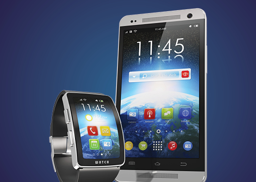
For the past few years, flip chip packages have dominated the mobile product market. The industry is notoriously resistant to replacing incumbent technology unless there are significant improvement gains, either performance or cost. FOWLP enables thinner packages and higher densities, which aligns well with mobile device makers, as well as IoT products. It is also a lower-cost alternative to 3D TSVs, and may push out 3D adoption in consumer applications a bit further, or displace them altogether. Additionally, as CMOS scaling to smaller nodes continues, we are reaching the limits of scaling at the printed circuit board end, which is creating a feature-size gap that current FOWLP and emerging high-density FO technologies like InFO are designated to fill. As we know, it is widely thought that FOWLP will make its first large-scale appearance in mobile electronics this year, which could be the inflection point that takes FOWLP into high-volume manufacturing.
While FOWLP and other emerging HD advanced packages may fill the gap in consumer electronics, we believe 2.5D and 3D IC technologies will fill it on the server side. Mobile devices are reliant on the cloud—essentially a network of servers needed to store and manage enormous quantities of data. While we are improving mobile technology, we also need to be improving the cloud infrastructure. As the server market is tilted more heavily toward being performance driven versus cost driven, this makes a compelling argument for 3D packaging.
All of this momentum behind FOWLP, 2.5D and 3D technologies is driving increased requirements for new, improved, materials. Different approaches may require different materials, and we must be ready to support them all, which is a challenge. Customization happens mostly at the technology level and involves subtle differences. We need to be ready to accommodate the regular “annual ordering patterns” to hit the schedules. While this creates uncertainty, it also brings opportunity, and Dow Electronic Materials is well positioned to take on these challenges, thanks in part to a long history in all the different areas.
After several somewhat-tentative years, the motivation for device pervasiveness and the creation of a connected world is creating high expectations for 2016 and beyond for advanced packaging innovation. These are truly exciting times as we tackle these new material challenges.