Dow Electronic Materials recently announced that three of its products have been selected as finalists for the 2015 R&D 100 Awards, which celebrate the most significant technology inventions of the past year. The winners will be announced Nov. 13, 2015, during a ceremony at Caesar’s Palace in Las Vegas. In this three-part interview series, we go behind the scenes with Dow experts who played pivotal roles in the development and commercialization of these innovative chemistries.
In part one of this series, Maria Rzeznik, Interconnect Technologies (IT) R&D Director for Americas and EMEA, talks about the changing requirements in high-density printed circuit boards (PCBs) driven by portable consumer electronics, and how MICROFILL™ THF-100 Electrolytic Copper is addressing them.
Why is the industry transitioning from conventional plating to through-hole super filling in manufacturing high-density PCBs?
Portable consumer electronics have become the primary driver for the ever-increasing circuit density of today’s printed circuit designs. Based on the small dimensions of these devices, through-hole and blind via diameters are typically in the 75μm to 150μm range. Performance improvement and process cost reduction make through-hole filling technology with copper an excellent approach, rather than the conventional-plated through-hole process. Super-filling electrodeposition of Cu in microvias and through-holes provides a means to achieve the required wiring densities and reliability demands. Both of these processes are preferred over via and through-hole conformal plating approaches, not only due to better productivity, but also more particularly for the cost savings and excellent board reliability they offer.
Why was MICROFILL™ developed?
The IC packaging industry was looking for a through-hole filling technology that would provide improved throughput, reliability and surface distribution for Cu electroplating. This plating can’t be done without a novel, well-balanced additive package, which is the foundation of MICROFILL™. This is a good example of how novel materials developed by Dow are designed to meet the challenges of smaller design features, thereby enabling smaller PCBs.
What is it about MICROFILL™ that makes it so innovative, and what challenges does it overcome?
What makes MICROFILL™ innovative is that it allows customers to replace a labor-intensive multistep process with a single Cu plating process.
Substrates for such applications were electroplated with a conventional conformal through hole process, then plugged with an epoxy material. Then, additional planarization, re-metallization and electrolytic-copper capping steps were required before buildup process steps could begin.
By carefully selecting the right balance of inorganic and organic additives along with design and synthesis of the right leveler additive, Dow Electronic Materials has been able to provide a “single chemistry does it all” process that, in combination with optimized plating conditions and plating equipment, is compatible with all through-hole geometries.
MICROFILL™ THF-100 Electrolytic Copper eliminates the need for conductive paste, inks, and solvents used in the conventional process, which reduces cost and improves productivity. It forms planar, solid Cu plug resulting in reduced CTE mismatch within filled via structures. Compared to conventional via fill processes, this new technology provides excellent copper-to-copper adhesion resulting in improved reliability, and both electrical and thermal conductivity.
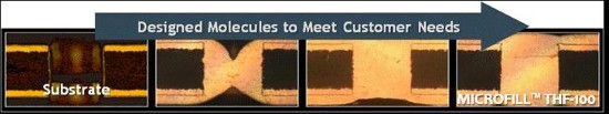
Through Hole Fill Plating Process with MICROFILL™ THF-100 Electrolytic Copper
MICROFILL™ THF-100 Electrolytic Copper technology is a significant advance over conventional hold plug processes. Steps using the MICROFILL™ THF-100 process are shown in the bottom sequence. Once step replaces the four steps in the conventional process, shown in the top panel. This eliminates steps and reagents, yielding a superior product in less processing time.
How is MICROFILL™ enhancing manufacturing and meeting next-generation requirements?
As we proceed from one generation to the next, circuit board complexity will continue to evolve. Portable and mobile computer electronics are drivers for designs that have improved performance, yet require reduced process costs.
The need for increased circuit densification and miniaturization, better performance and cost effectiveness will make it increasingly more challenging to balance both via filling and through hole plating requirements. These requirements include through hole plating at higher plating rates for increased productivity and highly planar via fill, with minimum possible surface copper deposition. As circuit board complexity continues to evolve, new additive development and formulation modification will evolve to meet the demands of increased complexity and increased production throughput. Next Generation product development is underway to meet those demands.